
Activities of the NFSMM group in the RF&Microwave Laboratory

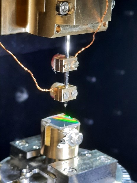
Positioning of a sample for electrical measurement using our home-built near-field scanning microwave microscope
Characterization of Material Parameters at Micron and Submicron Scales
Near field scanning microwave microscopy (NFSMM or shorter just SMM) is a fairly novel measurement technique within the family of scanning probe microscopy (SPM) that probes the device under test with a high frequency electromagnetic wave using a vector network analyzer (VNA). With an NFSMM one can measure simultaneously surface topography and electromagnetic properties of materials with sub-micrometer resolution. METAS is active in this area since 2011. As of today we are operating a home-built NFSMM and have participated in various projects to test the applicability of the NFSMM for a variety of measurement tasks. We characterized a wide range of materials, such as doped III-V semiconductors, battery cells, solar cells, nanostructured materials, nano devices, 2D materials and piezoelectric materials. Most importantly, we also developed new calibration algorithms allowing for quantitative measurements with uncertainties.
If you are interested in characterizing electrical properties of your samples/devices (frequency range between 0-50 GHz), please write to us at hf@metas.ch with a subject: "Characterize samples with NFSMM". A member of our team will get in touch with you.
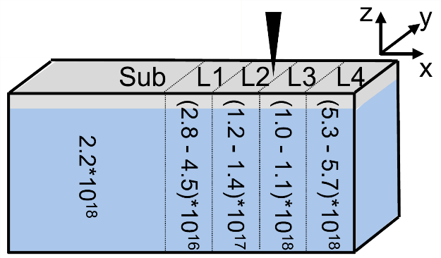
Scheme of n-doped GaAs staircase sample
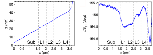
NFSMM cross section scan of n-doped GaAs staircase sample. Topography on the left, phase of S11 on the right.
Development of Impedance Standards for NFSMM
In contrast to the currently available calibration kits, which only include capacitive standards, METAS provides a complete set of standards, including capacitive, inductive and resistive circuits. With resistance and inductance between 0-960 Ohm and 0-1.15nH, respectively, and capacitive devices in the fF range.
If you are interested in these special calibration kits or would like to have your own customized ones, please write to us at hf@metas.ch with a subject: "Calibration standards for NFSMM". We are also providing consulting services on calibration standards design and fabrication.
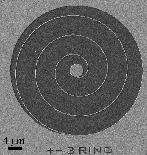
Impedance standard: top-view SEM image of a three-ring resistive/inductive structure.
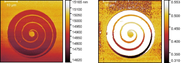
2d x-y scan with NFSMM of impedance standard. Shown are topography on the left and magnitude of S11 on the right
Development of coaxial probe for NFSMM
Currently the calibration of an NFSMM is in most practical use cases not transferable, which means: a tip calibrated with calibration standards on one sample cannot be used for quantitative measurements performed on another sample. This limits the applications of the NFSMM for quantitative measurements. METAS tries to overcome this limitation by using a coaxial tip. The objective is to achieve better shielding of parasitic electromagnetic fields and thus reduce their influence in performed measurements.
A coaxial probe mounted onto its holder. Two piezoelectric chrystals are attached to the coaxial probe, the upper one acting as a shaker, the lower one as a microphone providing the necessary feedback signal to control the distance between probe and sample.

Scanning electron microscopic (SEM) image taken of a coaxial probe after the pulling process. A short and sharp Pt wire (307 nm long and 95 nm wide) protrudes from the end of the borosilicate glass capillary. To enable SEM analysis of the tip, a thin gold layer was deposited on its surface.

Topography (top panel) and S11 signals (magnitude and phase: middle and bottom panels correspondingly) recorded by scanning the coaxial probe over an edge of a gold film deposited onto SiN film on a Si substrate. Arrows were added to mark jumps observed in both z and electrical signals by moving the probe from SiN (left) to Au (right) regions. Thanks to the shielding effect of the thick metallic outer conductor, regions away from the edge stays flat and homogeneous. In order to protect the probe, instead of having it in contact constantly with the sample, we retract and land it between two measured pixels.

2D map of S11 phase recorded on a test sample with a conventional tip, which contains a 50 nm thick gold structure deposited onto SiN film. A similar contrast is also observed for the amplitude of S11 signal.

User-friendly GUI developed at METAS using Python and the Qt framework.
If you have plans to build your own NFSMM system, do not hesitate to contact us at hf@metas.ch with a subject: "Development of NFSMM". An NFSMM matching your requirements can be designed, assembled, tested and installed for you. Consulting services are also available.
Development of a multi sensor device
One of the main drawbacks of NFSMM and of most SPM systems in general, which limits its use in industrial environment, is the time required to approach the tip to the sample and to scan over a small region of interest. To tackle this issue, in the Nanobat project, we are aiming to develop a new scan device, which has multiple metallic probes and possess a much higher speed (20 seconds for approach and scanning a 300umx300um region with 2um resolution). In the first prototype, the number of sensors is only four, but this number can be increased in future systems.
Selected publications
Advanced calibration kit for scanning microwave microscope: Design, fabrication and measurement
T. Le Quang, A. C. Grungor, D. Vasyukov, J. Hoffmann, J. Smajic and M. Zeier, Review of Scientific Instruments, 92, 023705 (2021).
Fabrication and measurements of inductive devices for Scanning microwave microscopy
T. Le Quang, D. Vasyukov, J. Hoffmann, A. Buchter and M. Zeier, 19th IEEE Conference on Nanotechnology, Macau, Conference Publication, 2019.
Scanning microwave microscopy applied to semiconducting GaAs structures
A. Buchter, J. Hoffmann, A. Delvallée, E. Brinciotti, D. Hapiuk, C. Licitra, K. Louarn, A. Arnoult, G. Almuneau, F. Piquemal, M. Zeier, F. Kienberger; Review of Scientific Instruments 89 (2018) 023704
Measuring Low Loss Dielectric Substrates with Scanning Probe Microscopes
J. Hoffmann, G. Gramse, J. Niegemann, M. Zeier, F. Kienberger; Applied Physics Letters, Vol 105, Issue 1, pp 013102 - 013102-4, July 2014
A Calibration Algorithm for Near field Scanning Microwave Microscopes
J. Hoffmann, M. Wollensack, M. Zeier, J. Niegemann, H.P. Huber, F. Kienberger; 12th IEEE Conference on Nanotechnology, Birmingham, Conference Publication, 2012
Projects
Last modification 24.09.2024


Contact
Federal Institute of Metrology
Laboratory RF and Microwave
Lindenweg 50
CH-3003
Bern-Wabern
T
+41 58 387 01 11